TCLK5
|
|
LCDDAT18|TIOA1
|
MCI2_DA1
|
PC12
<thead>
| 6 |
</thead>
<tbody>
| 7 |
| PC3 |
| ERX1 |
</tbody>
|
TIOA4
|
|
LCDDAT21|PCK2
|
MCI2_CK
|
PC15
<thead>
| 8 |
</thead>
<tbody>
| 9 |
| PC6 |
| ERXER |
</tbody>
|
TIOA5
|
|
LCDDAT17|TIOB1
|
MCI2_DA2
|
PC13
<thead>
| 10 |
</thead>
<tbody>
| 11 |
| PC4 |
| ETXEN |
</tbody>
|
TIOB4
|
|
LCDDAT20
|
MCI2_CDA
|
PC10
<thead>
| 12 |
</thead>
<tbody>
| 13 |
| PC7 |
| EREFCK |
</tbody>
|
TIOB5
|
|
LCDDAT16|TCLK1
|
MCI2_DA3
|
PC14
<thead>
| 14 |
</thead>
<tbody>
| 15 |
| PC0 |
| ETX0 |
</tbody>
|
TIOA3
|
|
|
SSC0
|
RK0
|
PC19
<thead>
| 16 |
</thead>
<tbody>
| 17 ||PC2 ||ERX0 ||TCLK3 || || ||TF0 ||PC17 ||18 |
| - |
| 19 |
| PC5 |
| ECRSDV |
</tbody>
|
TCLK4
|
|
|
RF0
|
PC20
<thead>
| 20 |
</thead>
<tbody>
| 21 |
| PC9 |
| EMDIO |
</tbody>
|
|
|
|
RD0
|
PC21
<thead>
| 22 |
</thead>
<tbody>
| 23 |
| PC30 |
| UTXD0 |
| rowspan=2|UART0 |
| ISI_PCK |
| |
| |
</tbody>
|
TK0
|
PC16
<thead>
| 24 |
</thead>
<tbody>
| 25 |
| PC29 |
| URXD0 |
</tbody>
|
ISI_D8|PWMFI2
|
|
|
TD0
|
PC18
<thead>
| 26 |
</thead>
<tbody>
| 27 |
| GND_POWER |
| |
| |
| |
| |
| |
| |
| |
| GND_POWER |
| 28 |
| - |
| 29 |
| PC31 |
| |
| |
| PWMFI1|FIQ |
| |
| |
| rowspan=2|LCDC |
| LCDVSYNC |
| PA26 |
| 30 |
| - |
| 31 ||PC23 ||SPI1_MOSI ||rowspan=5|SPI1 || || || ||LCDDISP ||PA25 ||32 |
| - |
| 33 ||PC25 ||SPI1_NPCS0 || || || || || ||GND_POWER ||34 |
| - |
| 35 ||PC22 ||SPI1_MISO || || || ||LCDC ||LCDHSYNC ||PA27 ||36 |
| - |
| 37 ||PC24 ||SPI1_SPCK || || || || || ||GND_POWER ||38 |
| - |
| 39 ||PC28 ||SPI1_NPCS3 ||ISI_D9|PWMFI0 || || ||rowspan=15|LCDC ||LCDDEN ||PA29 ||40 |
| - |
| 41 ||PA4 ||LCDDAT4 ||rowspan=12|LCDC || || || ||LCDDAT2 ||PA2 ||42 |
| - |
| 43 ||PA10 ||LCDDAT10 || || || ||LCDDAT15 ||PA15 ||44 |
| - |
| 45 ||PA14 ||LCDDAT14 || || ||ISI_D1 ||LCDDAT17 ||PA17 ||46 |
| - |
| 47 ||PA12 ||LCDDAT12 || || || ||LCDDAT1 ||PA1 ||48 |
| - |
| 49 ||PA24 ||LCDPWM || || || ||LCDDAT0 ||PA0 ||50 |
| - |
| 51 ||PA22 ||LCDDAT22 ||ISI_D6|PWMH1 || || ||LCDDAT3 ||PA3 ||52 |
| - |
| 53 ||PA28 ||LCDPCK || || || ||LCDDAT8 ||PA8 ||54 |
| - |
| 55 ||PA20 ||LCDDAT20 ||ISI_D4|PWMH0 || || ||LCDDAT6 ||PA6 ||56 |
| - |
| 57 ||PA21 ||LCDDAT21 ||ISI_D5|PWML0 || ||ISI_D2|TWD2 ||LCDDAT18 ||PA18 ||58 |
| - |
| 59 ||PA23 ||LCDDAT23 ||ISI_D7|PWML1 || ||ISI_D0 ||LCDDAT16 ||PA16 ||60 |
| - |
| 61 ||PA5 ||LCDDAT5 || || ||ISI_D3|TWCK2 ||LCDDAT19 ||PA19 ||62 |
| - |
| 63 ||PA7 ||LCDDAT7 || || || ||LCDDAT11 ||PA11 ||64 |
| - |
| 65 ||PA30 ||TWD0 ||rowspan=2|TWI0 ||URXD1|ISI_VSYNC || || ||LCDDAT9 ||PA9 ||66 |
| - |
| 67 ||PA31 ||TWCK0 ||UTXD1|ISI_HSYNC || || ||LCDDAT13 ||PA13 ||68 |
| - |
| 69 ||PD31 || || ||PCK1|AD11 || ||ISI_D10|SPI1_NPCS2 ||rowspan=2|TWI1 ||TWCK1 ||PC27 ||70 |
| - |
| 71 ||PD30 ||PCK0 ||SSC0:CLK ||AD10 || ||ISI_D11|SPI1_NPCS1 ||TWD1 ||PC26 ||72 |
| - |
| 73 ||PD29 ||AD9 ||rowspan=10|AD || || || ||rowspan=8|MCI0 ||MCI0_DA3 ||PD4 ||74 |
| - |
| 75 ||PD28 ||AD8 || || || ||MCI0_DA1 ||PD2 ||76 |
| - |
| 77 ||PD27 ||AD7 || || || ||MCI0_CDA ||PD0 ||78 |
| - |
| 79 ||PD26 ||AD6 || || || ||MCI0_CK ||PD9 ||80 |
| - |
| 81 ||PD23 ||AD3 || || || ||MCI0_DA2 ||PD3 ||82 |
| - |
| 83 ||PD22 ||AD2 || || || ||MCI0_DA0 ||PD1 ||84 |
| - |
| 85 ||PD24 ||AD4 || || ||PWML2|TIOB0 ||MCI0_DA5 ||PD6 ||86 |
| - |
| 87 ||PD21 ||AD1 || || ||PWML3 ||MCI0_DA7 ||PD8 ||88 |
| - |
| 89 ||PD25 ||AD5 || || ||SPI0_NPCS2|CTS0 ||rowspan=2|CAN0 ||CANTX0 ||PD15 ||90 |
| - |
| 91 ||PD20 ||AD0 || || ||SPI0_NPCS1|SCK0 ||CANRX0 ||PD14 ||92 |
| - |
| 93 ||PD5 ||PWMH2 ||rowspan=2|PWM ||MCI0_DA4|TIOA0 || || ||UART0 ||TXD0 ||PD18 ||94 |
| - |
| 95 ||PD7 ||PWMH3 ||MCI0_DA6|TCLK0 || || || ||RXD0 ||PD17 ||96 |
| - |
| 97 ||PD19 || ||GPIO ||ADTRG || || ||rowspan=3|SPI0 ||SPI0_MISO ||PD10 ||98 |
| - |
| 99 ||PB0 ||GTX0 ||rowspan=15|GMAC ||PWMH0 || || ||SPI0_SPCK ||PD12 ||100 |
| - |
| 101 ||PB7 ||GRX3 ||RK1 || || ||SPI0_MOSI ||PD11 ||102 |
| - |
| 103 ||PB13 ||GRXER ||PWML3 || ||PWMH3|GRXDV ||GMAC:INTRP || ||PB12 ||104 |
| - |
| 105 ||PB17 ||GMDIO || || ||GCOL ||rowspan=2|CAN0 ||CANTX1 ||PB15 ||106 |
| - |
| 107 ||PB11 ||GRXCK ||RD1 || ||GCRS ||CANRX1 ||PB14 ||108 |
| - |
| 109 ||PB18 ||G125CK || || ||GTX7 ||rowspan=6|MCI1 ||MCI1_DA2 ||PB22 ||110 |
| - |
| 111 ||PB1 ||GTX1 ||PWML0 || ||GRX5 ||MCI1_CK ||PB24 ||112 |
| - |
| 113 ||PB4 ||GRX0 ||PWMH1 || ||GTX5 ||MCI1_DA0 ||PB20 ||114 |
| - |
| 115 ||PB3 ||GTX3 ||TF1 || ||GTX6 ||MCI1_DA1 ||PB21 ||116 |
| - |
| 117 ||PB8 ||GTXCK ||PWMH2 || ||GTX4 ||MCI1_CDA ||PB19 ||118 |
| - |
| 119 ||PB9 ||GTXEN ||PWML2 || ||GRX4 ||MCI1_DA3 ||PB23 ||120 |
| - |
| 121 ||PB2 ||GTX2 ||TK1 || ||G125CKO ||rowspan=4|USART1 ||RTS1 ||PB27 ||122 |
| - |
| 123 ||PB6 ||GRX2 ||TD1 || || ||RXD1 ||PB28 ||124 |
| - |
| 125 ||PB5 ||GRX1 ||PWML1 || || ||TXD1 ||PB29 ||126 |
| - |
| 127 ||PB16 ||GMDC || || ||GRX7 ||CTS1 ||PB26 ||128 |
| - |
| 129 ||PB25 || || ||SCK1|GRX6 || ||RF1|GTXER ||EMAC:INT_N || ||PB10 ||130 |
| - |
| 131 ||BMS || || || || || || || ||DIBN ||132 |
| - |
| 133 ||NRST || || || || || || || ||DIBP ||134 |
| - |
| 135 ||TDI || || || || || ||rowspan=2|DEBUG ||DTXD ||PB31 ||136 |
| - |
| 137 ||JTAGSEL || || || || || ||DRXD ||PB30 ||138 |
| - |
| 139 ||TCK ||SWCLK || || || ||PWMFI3|SPI0_NPCS3|RTS0 ||SSC0:IRQ || ||PD16 ||140 |
| - |
| 141 ||TMS ||SWDIO || || || || || || ||GND_POWER ||142 |
| - |
| 143 ||TDO || || || || || ||USBA ||DHSDP ||HHSDPA ||144 |
| - |
| 145 ||NTRST || || || || || || ||DHSDM ||HHSDMA ||146 |
| - |
| 147 ||WKUP || || || || || ||USBB || ||HHSDPB ||148 |
| - |
| 149 ||SHDN || || || || || || || ||HHSDMB ||150 |
| - |
| 151 ||D7 || ||rowspan=8|EBI:Dx || || || ||USBC || ||HHSDMC ||152 |
| - |
| 153 ||D6 || || || || || || ||HHSDPC ||154 |
| - |
| 155 ||D5 || || || ||LCDDAT23|TIOB2 ||rowspan=10|EBI ||NCS2 ||PE28 ||156 |
| - |
| 157 ||D4 || || || ||LCDDAT22|TIOA2 ||NCS1 ||PE27 ||158 |
| - |
| 159 ||D3 || || || ||USART2:CTS2 ||A23 ||PE23 ||160 |
| - |
| 161 ||D2 || || || ||USART2:RXD2 ||A25 ||PE25 ||162 |
| - |
| 163 ||D1 || || || ||USART2:TXD2 ||NCS0 ||PE26 ||164 |
| - |
| 165 ||D0 || || || || ||A20 ||PE20 ||166 |
| - |
| 167 ||PE3 ||A3 ||rowspan=11|EBI:Ax ||GPIO:LED || ||USART2:RTS2 ||A24 ||PE24 ||168 |
| - |
| 169 ||PE5 ||A5 || || ||TCLK2 ||NWR1/NBS1 ||PE29 ||170 |
| - |
| 171 ||PE6 ||A6 || || ||USART3:RXD3 ||A18 ||PE18 ||172 |
| - |
| 173 ||PE13 ||A13 || || ||USART3:TXD3 ||A19 ||PE19 ||174 |
| - |
| 175 ||PE15 ||A15 ||SCK3 || ||PWML1|IRQ ||MMC1:VDD_EN || ||PE31 ||176 |
| - |
| 177 ||PE8 ||A8 || || ||NWAIT ||MMC1:CD || ||PE30 ||178 |
| - |
| 179 ||PE10 ||A10 || || ||GPIO:LED ||rowspan=7|EBI:Ax ||A4 ||PE4 ||180 |
| - |
| 181 ||PE14 ||A14 || || ||GPIO:LED ||A2 ||PE2 ||182 |
| - |
| 183 ||PE16 ||A16 ||CTS3 || ||GPIO:LED ||A1 ||PE1 ||184 |
| - |
| 185 ||PE0 ||A0/NBS0 || || || ||A7 ||PE7 ||186 |
| - |
| 187 ||PE11 ||A11 || || ||RTS3 ||A17 ||PE17 ||188 |
| - |
| 189 ||GND_POWER || || || || || ||A9 ||PE9 ||190 |
| - |
| 191 ||GND_POWER || || || || || ||A12 ||PE12 ||192 |
| - |
| 193 ||GND_POWER || || || || || || || ||VCC_3V3 ||194 |
| - |
| 195 ||GND_POWER || || || || || || || ||VCC_3V3 ||196 |
| - |
| 197 ||GND_POWER || || || || || || || ||VCC_3V3 ||198 |
| - |
| 199 ||GND_POWER || || || || || || || ||VCC_3V3 ||200 |
| - |
| colspan=11|说明1:“可复用的信号”栏中黄色背景表示在MY-SAMA5-EK200上实现的信号。 |
| - |
| colspan=11|说明2:MY-SAMA5-CB200-D36引出的管脚主要有PA0~PA31、PB0~PB31、PC0~PC31、PD0~PD12、PD14~PD31、PE0~PE20、PE23~PE31。 |
| } |
</tbody>
= SAMA5D3 MPU介绍 =
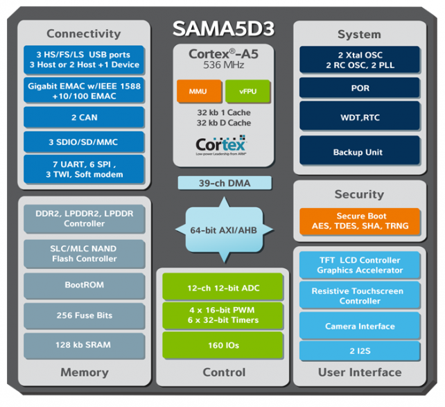
SAMA5关键亮点
高性能
SAMA5 系列是专为弥补 ARM Cortex-A5 内核在功率方面的不足而设计,包括的器件能以低至 150 mW 的功耗提供高达 945DMIPS 的处理能力。
- 1.58 DMIPS/MHz ARM Cortex-A5 内核
- 高达 600 MHz 的最大工作频率 (945DMIPS)
- 64 位内部总线架构、可提供高达 1600 MB/s 带宽的 32 位宽 DDR 控制器
- 用于高精度计算和快速数据处理的 Neon 和浮点运算单元 (FPU)
- ARM Cortex-A5 FPU 的性能是 ARM Cortex-A8 FPU 的三倍
- L2 缓存,用于提高整体系统性能
低功耗
SAMA5 器件采用创新技术以降低所有模式下的功耗,并且可实现:
- 在激活所有外设的情况下,以低于 150mW 的功耗(在工作模式下)提供高达 536MHz 的工作频率
- 在运行 SRAM 和 寄存器保留的低功耗模式下,功耗低于 0.5mW 且唤醒时间短于 0.5ms。在运行 RTC(实时时钟)的备份模式下功耗约为 1.2µA
连接性
SAMA5 器件嵌入了各种高级通信外设,因此是网桥和网关的理想之选。
- 支持 IEEE1588 的以太网 MAC 和千兆位以太网 MAC、双 CAN 端口
- 可配置为三个主机或两个主机及一个器件端口的三个高速 USB 端口
- 多个 SDIO/SD/MMC 端口、UART、SPI、TWI、软调制解调器、CMOS 图像传感器接口、ADC、32 位定时器等。有关更多详细信息,请参阅“器件概述”选项卡
增强的用户界面
使用 SAMA5 MPU,可以创建当今应用所需的时尚、平稳的用户界面。
- 图形 LCD 控制器具有图像合成叠加和集成功能(如 α 混合、缩放、颜色转换和旋转)
- 720p 硬件视频解码器,用于加快支持当今主流视频标准的视频回放
- 电阻式触摸屏界面
- CMOS 图像传感器接口
安全
SAMA5 系列包括防止克隆、确保真实性以及保护应用的通信和数据存储安全的功能。
- 安全引导
- 硬件加密引擎,如高级加密标准 (AES)/三重数据加密标准 (DES)、RSA (Rivest-Shamir-Adleman) 和 ECC(椭圆曲线加密)以及安全哈希算法 (SHA) 和真正的随机号码生成器 (TRNG)
- 通过外部 DDR 内存即时加密/解密代码
- 管脚篡改检测,以保护系统免受物理入侵
- 密钥和数据的安全存储
- ARM 信任区域,用于对系统、外设和内存资源进行分区,以将安全关键型软件与开放环境操作系统隔离
安全性
SAMA5 系列具有的功能可轻松简便地实施如 IEC61508 等安全标准。
- 主晶体振荡器时钟具有故障检测器
- 上电复位
- 独立的看门狗定时器
- 寄存器写保护
- 内存管理单元 (MMU) 允许在内存内设置区域保护
- 基于 SHA 的 ICM(完整性检查监控器),用于验证内存内容的完整性
低系统成本
SAMA5 凭借高度的系统集成,在实现最大灵活性的同时还减少了对其他昂贵组件的需求。
- 0.8mm 球间距封装简化了 PCB 设计并降低了成本
- 最低功耗方案,需要芯片离散的电源或低成本 PMIC
- 三个高速 USB 端口节省了外部集线器的成本
- DDR(双数据速率)内存线路上的阻抗控件节省了外部电阻器
- 嵌入式 RTC 节省了外部组件
- 集成的软调制解调器解决方案节省了外部调制解调器设备的成本
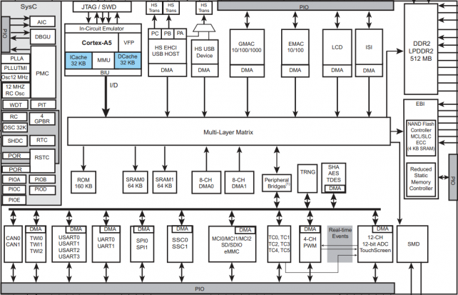
SAMA5D3 Features
Core
- ARM® Cortex®-A5 Processor with ARM v7-A Thumb2® Instruction Set
- CPU Frequency up to 536 MHz
- 32 Kbyte Data Cache, 32 Kbyte Instruction Cache, Virtual Memory System Architecture (VMSA)
- Fully Integrated MMU and Floating Point Unit (VFPv4)
Memories
- One 160 Kbyte Internal ROM Single-cycle Access at System Speed, Embedded Boot Loader: Boot on 8-bit
- NAND Flash, SDCard, eMMC, serial DataFlash®, selectable Order
- One 128 Kbyte Internal SRAM, Single-cycle Access at System Speed
- High Bandwidth 32-bit Multi-port Dynamic RAM Controller supporting 512 Mbyte 8 bank DDR2/LPDDR/LPDDR2 with datapath scrambling
- Independent Static Memory Controller with datapath scrambling and SLC/MLC NAND Support with up to 24-bit Error Correcting Code (PMECC)
System running up to 166 MHz
- Reset Controller, Shut Down Controller, Periodic Interval Timer, Watchdog Timer and Real-time Clock
- Boot Mode Select Option, Remap Command
- Internal Low-power 32 kHz RC Oscillator and Fast 12 MHz RC Oscillator
- Selectable 32768 Hz Low-power Oscillator and 12 MHz Oscillator
- One 400 to 1000 MHz PLL for the System and one PLL at 480 MHz optimize d for USB High Speed
- 39 DMA Channels including two 8-channel 64-bit Central DMA Controllers
- 64-bit Advanced Interrupt Controller
- Three Programmable External Clock Signals
- Programmable Fuse Box with 256 fuse bits, 192 of them available for Customer
Low Power Management
- Shut Down Controller
- Battery Backup Registers
- Clock Generator and Power Management Controller
- Very Slow Clock Operating Mode, Software Programmable Power Optimization Capabilities
Peripherals
- LCD TFT Controller with Overlay, Alpha-blending,Rotation, Scaling and Color Space Conversion
- ITU-R BT. 601/656 Image Sensor Interface
- Three HS/FS/LS USB Ports with On-Chip Transceivers
- One Device Controller
- One Host Controller with Integrated Root Hub (3 Downstream Ports)
- One 10/100/1000 Mbps Gigabit Ethernet MAC Controller (GMAC) with IEEE1588 support
- One 10/100 Mbps Ethernet MAC Controller (EMAC)
- Two CAN Controllers with 8 Mailboxes, fully Compliant with CAN 2.0 Part A and 2.0 Part B
- Softmodem Interface
- Three High Speed Memory Card Hosts (eMMC 4.3 and SD 2.0)
- Two Master/Slave Serial Peripheral Interfaces
- Two Synchronous Serial Controllers
- Three Two-wire Interface up to 400 Kbit/s supporting I2C Protocol and SMBUS
- Four USARTs, two UARTs, one DBGU
- Two Three-channel 32-bit Timer/Counters
- One 4-channel 16-bit PWM Controller
- One 12-channel 12-bit Analog-to-Digital Converter with Resistive Touch-Screen function
Safety
- Power-on Reset Cells
- Independent Watchdog
- Main Crystal Clock Failure Detection
- Write Protection Registers
- SHA: Supports Secure Hash Algorithm (SHA1, SHA224, SHA 256, SHA384, SHA512)
- Memory Management Unit
Security
- TRNG: True Random Number Generator
- Encryption Engine
- AES: 256-bit, 192-bit, 128-bit Key Algorithm, Compliant with FIPS PUB 197 Specifications
- TDES: Two-key or Three-key Algorithms, Co mpliant with FIPS PUB 46-3 Specifications
- Atmel® Secure Boot Solution
I/O
- Five 32-bit Parallel Input/Output Controllers
- 160 I/Os
- Input Change Interrupt Capability on Each I/O Line, Selectable Schmitt Trigger Input
- Individually Programmable Open-drain, Pull-up and Pull-down Resistor, Synchronous Output, Filtering
- Slew Rate Control on High Speed I/Os
- Impedance Control on DDR I/Os
Package
- 324-ball LFBGA, 15 x 15 x 1.4 mm, pitch 0.8 mm
- 324-ball TFBGA, 12 x 12 x 1.2 mm, pitch 0.5 mm
SAMA5D3 Embedded Characteristics
WDT
- 12-bit key-protected programmable counter
- Watchdog Clock is independent from Processor Clock
- Provides reset or interrupt signals to the system
- Counter may be stopped while the processor is in debug state or in idle mode
RTC
- Ultra Low Power Consumption
- Full Asynchronous Design
- Gregorian Calendar up to 2099
- Programmable Periodic Interrupt
- Safety/security features:
- Valid Time and Date Programmation Check
PIO
- Up to 32 Programmable I/O Lines
- Fully Programmable through Set/Clear Registers
- Multiplexing of Four Peripheral Functions per I/O Line
- For each I/O Line (Whether Assigned to a Peripheral or Used as General Purpose I/O)
- Input Change Interrupt
- Programmable Glitch Filter
- Programmable Debouncing Filter
- Multi-drive Option Enables Driving in Open Drain
- Programmable Pull-Up on Each I/O Line
- Pin Data Status Register, Supplies Visibility of the Level on the Pin at Any Time
- Additional Interrupt Modes on a Programmable Event: Rising Edge, Falling Edge, Low-Level or High-Level
- Lock of the Configuration by the Connected Peripheral
- Synchronous Output, Provides Set and Clear of Several I/O Lines in a Single Write
- Register Write Protection
- Programmable Schmitt Trigger Inputs
- Programmable I/O Drive
LCDC
- Dual AHB Master Interface
- Supports Single Scan Active TFT Display
- Supports 12-, 16-, 18- and 24-bit Output Mode through the Spatial Dithering Unit
- Asynchronous Output Mode Supported (at synthesis time)
- 1, 2, 4, 8 bits per pixel (palletized)
- 12, 16, 18, 19, 24, 25 and 32 bits per pixel (non palletized)
- Supports One Base Layer (background)
- Supports Two Overlay Layer Windows
- Supports One High End Overlay (HEO) Window
- Supports One Hardware Cursor, Fixed or Free Size
- Hardware Cursor Fixed Size on the following patterns: 32x32, 64x64 and 128x128
- Little Endian Memory Organization
- Programmable Timing Engine, with Integer Clock Divider
- Programmable Polarity for Data, Line Synchro and Frame Synchro.
- Display Size up to 2048x2048, or up to 720p in video format
- Color Lookup Table with up to 256 entries and Predefined 8-bit Alpha
- Programmable Negative and Positive Row Striding for all Layers
- Programmable Negative and Positive Pixel Striding for all Overlay1, Overlay2 and HEO layers
- High End Overlay supports 4:2:0 Planar Mode and Semiplanar Mode
- High End Overlay supports 4:2:2 Planar Mode, Semiplanar Mode and Packed
- High End Overlay includes Chroma Upsampling Unit
- Horizontal and Vertical Rescaling unit with Edge Interpolation and Independent Non Integer Ratio
- Hidden Layer Removal supported.
- Integrates Fully Programmable Color Space Conversion
- Overlay1, Overlay2 and High End Overlay Integrate Rotation Engine: 90, 180, 270
- Blender Function Supports Arbitrary 8-bit Alpha Value and Chroma Keying
- DMA User interface uses Linked List Structure and Add-to-queue Structure
ISI
- ITU-R BT. 601/656 8-bit Mode External Interface Support
- Supports up to 12-bit Grayscale CMOS Sensors
- Support for ITU-R BT.656-4 SAV and EAV Synchronization
- Vertical and Horizontal Resolutions up to 20482048
- Preview Path
- Up to 2048*2048 in Grayscale Mode
- Up to 640480 in RGB Mode
- 32 Bytes FIFO on Codec Path
- 32 Bytes FIFO on Preview Path
- Support for Packed Data Formatting for YCbCr 4:2:2 Formats
- Preview Scaler to Generate Smaller Size image
- Programmable Frame Capture Rate
- VGA, QVGA, CIF, QCIF Formats Supported for LCD Preview
- Custom Formats with Horizontal and Vertical Preview Size as Multiples of 16 Also Supported for LCD Preview
UDPHS
- 1 Device High Speed
- 1 UTMI transceiver shared between Host and Device
- USB v2.0 High Speed Compliant, 480 Mbit/s
- 16 Endpoints up to 1024 bytes
- Embedded Dual-port RAM for Endpoints
- Suspend/Resume Logic (Command of UTMI)
- Up to Three Memory Banks for Endpoints (Not for Control Endpoint)
- 8 KBytes of DPRAM
UHPHS
- Compliant with Enhanced HCI Rev 1.0 Specification
- Compliant with USB V2.0 High-speed
- Supports High-speed 480 Mbps
- Compliant with OpenHCI Rev 1.0 Specification
- Compliant with USB V2.0 Full-speed and Low-speed Specification
- Supports both Low-speed 1.5 Mbps and Full-speed 12 Mbps USB devices
- Root Hub Integrated with 3 Downstream USB HS Ports
- Embedded USB Transceivers
- Supports Power Management
- Hosts (A and B) High Speed (EHCI), Port A shared with UDPHS
GMAC
- Compatible with IEEE Standard 802.3
- 10, 100 and 1000 Mbps operation
- Full and half duplex operation at all supported speeds of operation
- Statistics Counter Registers for RMON/MIB
- MII/GMII/RGMII interface to the physical layer
- Integrated physical coding
- Direct memory access (DMA) interface to external memory
- Programmable burst length and endianism for DMA
- Interrupt generation to signal receive and transmit completion, or errors
- Automatic pad and cyclic redundancy check (CRC) generation on transmitted frames
- Frame extension and frame bursting at 1000 Mbps in half duplex mode
- Automatic discard of frames received with errors
- Receive and transmit IP, TCP and UDP checksum offload. Both IPv4 and IPv6 packet types supported
- Address checking logic for four specific 48-bit addresses, four type IDs, promiscuous mode, hash matching of
- unicast and multicast destination addresses and Wake-on-LAN
- Management Data Input/Output (MDIO) interface for physical layer management
- Support for jumbo frames up to 10240 bytes
- Full duplex flow control with recognition of incoming pause frames and hardware generation of transmitted pause
- frames
- Half duplex flow control by forcing collisions on incoming frames
- Support for 802.1Q VLAN tagging with recognition of incoming VLAN and priority tagged frames
- Support for 802.1Qbb priority-based flow control
- Programmable Inter Packet Gap (IPG) Stretch
- Recognition of IEEE 1588 PTP frames
- IEEE 1588 time stamp unit (TSU)
- Support for 802.1AS timing and synchronization
EMAC
- Supports RMII Interface to the physical layer
- Compatible with IEEE Standard 802.3
- 10 and 100 Mbit/s Operation
- Full-duplex and Half-duplex Operation
- Statistics Counter Registers
- Interrupt Generation to Signal Receive and Transmit Completion
- DMA Master on Receive and Transmit Channels
- Transmit and Receive FIFOs
- Automatic Pad and CRC Generation on Transmitted Frames
- Automatic Discard of Frames Received with Errors
- Address Checking Logic Supports Up to Four Specific 48-bit Addresses
- Supports Promiscuous Mode Where All Valid Received Frames are Copied to Memory
- Hash Matching of Unicast and Multicast Destination Addresses
- Physical Layer Management through MDIO Interface
- Half-duplex Flow Control by Forcing Collisions on Incoming Frames
- Full-duplex Flow Control with Recognition of Incoming Pause Frames
- Support for 802.1Q VLAN Tagging with Recognition of Incoming VLAN and Priority Tagged Frames
- Multiple Buffers per Receive and Transmit Frame
- Wake-on-LAN Support
- Jumbo Frames Up to 10240 bytes Supported
HSMCI
- Compatible with MultiMedia Card Specification Version 4.3
- Compatible with SD Memory Card Specification Version 2.0
- Compatible with SDIO Specification Version 2.0
- Compatible with CE-ATA Specification 1.1
- Cards Clock Rate Up to Master Clock Divided by 2
- Boot Operation Mode Support
- High Speed Mode Support
- Embedded Power Management to Slow Down Clock Rate When Not Used
- Supports 1 Multiplexed Slot(s)
- Each Slot for either a High Speed MultiMedia Card Bus (Up to 30 Cards) or an SD Memory Card
- Support for Stream, Block and Multi-block Data Read and Write
- Supports Connection to DMA Controller (DMAC)
- Minimizes Processor Intervention for Large Buffer Transfers
- Built in FIFO (from 16 to 256 bytes) with Large Memory Aperture Supporting Incremental Access
- Support for CE-ATA Completion Signal Disable Command
- Protection Against Unexpected Modification On -the-Fly of the Configuration Registers
SPI
- Supports Communication with Serial External Devices
- Master Mode can drive SPCK up to peripheral clock (bounded by maximum bus clock divided by 2)
- Slave Mode operates on SPCK, asynchronously to Core and Bus Clock
- Four Chip Selects with External Decoder Support Allow Communication with Up to 15 Peripherals
- Serial Memories, such as DataFlash and 3-wire EEPROMs
- Serial Peripherals, such as ADCs, DACs, LCD Controllers, CAN Controllers and Sensors
- External Coprocessors
- Master or Slave Serial Peripheral Bus Interface
- 8-bit to 16-bit Programmable Data Length Per Chip Select
- Programmable Phase and Polarity Per Chip Select
- Programmable Transfer Delay Between Consecutive Transfers and Delay before SPI Clock per Chip Select
- Programmable Delay Between Chip Selects
- Selectable Mode Fault Detection
- Connection to DMA Channel Capabilities Optimizes Data Transfers
- One channel for the Receiver, One Channel for the Transmitter
TWI
- 3 TWIs
- Compatible with Atmel Two-wire Interface Serial Memory and I²C Compatible Devices
- One, Two or Three Bytes for Slave Address
- Sequential Read-write Operations
- Master, Multi-master and Slave Mode Operation
- Bit Rate: Up to 400 Kbit/s
- General Call Supported in Slave mode
- SMBUS Quick Command Supported in Master Mode
- Connection to DMA Controller (DMA) Channel Capabilities Optimizes Data Transfers
SSC
- Provides Serial Synchronous Communication Links Used in Audio and Telecom Applications
- Contains an Independent Receiver and Transmitter and a Common Clock Divider
- Interfaced with the DMA Controller (DMAC) to Reduce Processor Overhead
- Offers a Configurable Frame Sync and Data Length
- Receiver and Transmitter Can be Programmed to Start Automatically or on Detection of Different Events on the
- Frame Sync Signal
- Receiver and Transmitter Include a Data Signal, a Clock Signal and a Frame Synchronization Signal
DBGU
- System Peripheral to Facilitate Debug of Atmel® ARM®-based Systems
- Composed of Four Functions
- Two-pin UART
- Debug Communication Channel (DCC) Support
- Chip ID Registers
- ICE Access Prevention
- Implemented Features are USART Compatible
- Independent Receiver and Transmitter with a Common Programmable Baud Rate Generator
- Even, Odd, Mark or Space Parity Generation
- Parity, Framing and Overrun Error Detection
- Automatic Echo, Local Loopback and Remote Loopback Channel Modes
- Interrupt Generation
- Support for Two DMA Channels with Connection to Receiver and Transmitter
- Debug Communication Channel Support
- Offers Visibility of COMMRX and COMM TX Signals from the ARM Processor
- Interrupt Generation
- Identification of the Device Revision, Sizes of the Embedded Memories, Set of Peripherals
- Enables Software to Prevent System Access Through the ARM Processor’s ICE
- Prevention is Made by Asserting the NTRST Line of the ARM Processor’s ICE
UART
- Independent Receiver and Transmitter with a Common Programmable Baud Rate Generator
- Even, Odd, Mark or Space Parity Generation
- Parity, Framing and Overrun Error Detection
- Automatic Echo, Local Loopback and Remote Loopback Channel Modes
- Interrupt Generation
- Support for Two DMA Channels with Connection to Receiver and Transmitter
USART
- Programmable Baud Rate Generator
- 5- to 9-bit Full-duplex Synchronous or Asynchronous Serial Communications
- 1, 1.5 or 2 Stop Bits in Asynchronous Mode or 1 or 2 Stop Bits in Synchronous Mode
- Parity Generation and Error Detection
- Framing Error Detection, Overrun Error Detection
- MSB- or LSB-first
- Optional Break Generation and Detection
- By 8 or by 16 Over-sampling Receiver Frequency
- Optional Hardware Handshaking RTS-CTS
- Receiver Time-out and Transmitter Timeguard
- Optional Multidrop Mode with Address Generation and Detection
- RS485 with Driver Control Signal
- ISO7816, T = 0 or T = 1 Protocols for Interfacing with Smart Cards
- NACK Handling, Error Counter with Repetition and Iteration Limit
- IrDA Modulation and Demodulation
- Communication at up to 115.2 Kbps
- Master or Slave
- Serial Clock Programmable Phase and Polarity
- SPI Serial Clock (SCK) Frequency up to Internal Clock Frequency MCK/6
- Remote Loopback, Local Loopback, Automatic Echo
- Two DMA Controller Channels (DMAC)
- Offers Buffer Transfer without Processor Intervention
CAN
- Fully Compliant with CAN 2.0 Part A and 2.0 Part B
- Bit Rates up to 1 Mbit/s
- 8 Object Oriented Mailboxes with the Following Properties:
- CAN Specification 2.0 Part A or 2.0 Part B Programmable for Each Message
- Object Configurable in Receive (with Overwrite or Not) or Transmit Modes
- Independent 29-bit Identifier and Mask Defined for Each Mailbox
- 32-bit Access to Data Registers for Each Mailbox Data Object
- Uses a 16-bit Timestamp on Receive and Transmit Messages
- Hardware Concatenation of ID Masked Bitfields To Speed Up Family ID Processing
- 16-bit Internal Timer for Timestamping and Network Synchronization
- Programmable Reception Buffer Length up to 8 Mailbox Objects
- Priority Management between Transmission Mailboxes
- Autobaud and Listening Mode
- Low Power Mode and Programmable Wake-up on Bus Activity or by the Application
- Data, Remote, Error and Overload Frame Handling
- Write Protected Registers
PWM
- Channels
- Common Clock Generator Providing Thirteen Different Clocks
- A Modulo n Counter Providing Eleven Clocks
- Two Independent Linear Dividers Working on Modulo n Counter Outputs
- Independent 16-bit Counter for Each Channel
- Independent Complementary Outputs with 12-bit Dead-Time Generator (Also Called Dead-Band or Non-Overlapping Time) for Each Channel
- Independent Enable Disable Command for Each Channel
- Independent Clock Selection for Each Channel
- Independent Period, Duty-Cycle and Dead-Time for Each Channel
- Independent Double Buffering of Period, Duty-Cycle and Dead-Times for Each Channel
- Independent Programmable Selection of The Output Waveform Polarity for Each Channel
- Independent Programmable Center or Left Aligned Output Waveform for Each Channel
- Independent Output Override for Each Channel
- Independent Interrupt for Each Channel, at Each Period for Left-Aligned or Center-Aligned Configuration
- 2 2-bit Gray Up/Down Channels for Stepper Motor Control
- Synchronous Channel Mode
- Synchronous Channels Share the Same Counter
- Mode to Update the Synchronous Channels Registers after a Programmable Number of Periods
- 2 Independent Events Lines Intended to Synchronize ADC Conversions
- Programmable delay for Events Lines to delay ADC measurements
- 8 Comparison Units Intended to Generate Interrupts, Pulses on Event Lines
- 1 Programmable Fault/Break Inputs Providing an Asynchronous Protection of PWM Outputs
- 4 User Driven through PIO inputs
- PMC Driven when Crystal Oscillator Clock Fails
- ADC Controller Driven through Configurable Comparison Function
- Write Protected Registers
ADC
- 12-bit Resolution
- 1 MHz Conversion Rate
- Wide Range Power Supply Operation
- Selectable Single Ended or Differential Input Voltage
- Programmable Gain For Maximum Full Scale Input Range 0 - VDD
- Resistive 4-wire and 5-wire Touchscreen Controller
- Position and Pressure Measurement for 4-wire screens
- Position Measurement for 5-wire screens
- Average of up to 8 measures for noise filtering
- Programmable Pen Detection sensitivity
- Integrated Multiplexer Offering Up to 12 Independent Analog Inputs
- Individual Enable and Disable of Each Channel
- Hardware or Software Trigger
- External Trigger Pin
- Timer Counter Outputs (Corresponding TIOA Trigger)
- Internal Trigger Counter
- Trigger on Pen Contact Detection
- PWM Event Line
- Drive of PWM Fault Input
- DMA Support
- Possibility of ADC Timings Configuration
- Two Sleep Modes and Conversion Sequencer
- Automatic Wakeup on Trigger and Back to Sleep Mode after Conversions of all Enabled Channels
- Possibility of Customized Channel Sequence
- Standby Mode for Fast Wakeup Time Response
- Power Down Capability
- Automatic Window Comparison of Converted Values
|
