MYZR-SSD20X-MB096 Hardware Introduction
目录
- 1 Overview of interfaces
- 2 MYZR-SSD20X-MB096 backplane description
- 2.1 1. Backplane Power
- 2.2 2. Reset circuit
- 2.3 3. LED display circuit
- 2.4 4. RTC real time clock circuit
- 2.5 5. External TF card circuit
- 2.6 6. Ethernet circuit interface
- 2.7 7. USB circuit
- 2.8 8. 4G module circuit
- 2.9 9. MIPI circuit
- 2.10 10. WIFI module circuit
- 2.11 11. SPI/I2C/AUD/GPIO/IRN circuit
- 2.12 12. RS232/485 circuit
- 2.13 13. Debug serial port and programming interface
Overview of interfaces
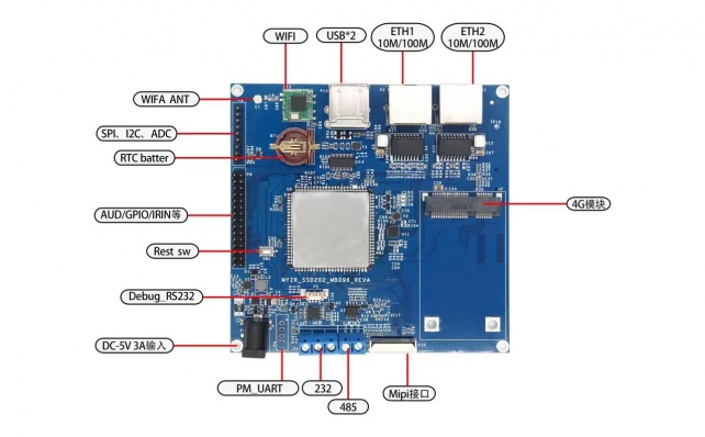
Front view
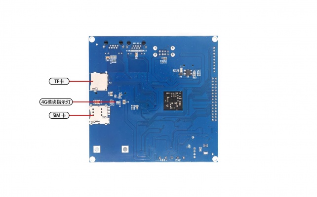
Rear view
MYZR-SSD20X-MB096 Baseplate parameters
| Number | Interface | Features | Interface form | Silkscreen |
|---|---|---|---|---|
| 1 | 5V_IN | power input | DC-005 round mouth | P1 |
| 2 | Ethernet | one 10/100M Ethernet | RJ45 | P2和P11 |
| 3 | DEBUG UART | Debug serial port | PH1.25 female header(4 Pin) | P5 |
| 4 | RS232 | RS232 interface | screw terminals | P6 |
| 5 | RS485 | RS485 interface | screw terminals | P7 |
| 6 | 4G module | 4G module interface | MINI-PCIE | J2 |
| 7 | sim | sim card | MICRO SIM self-propelled | J1 |
| 8 | TF | TF card | Standard TF card self-elastic deck | P3 |
| 9 | USB | USB2.0 | Double layer USB_A | P12 |
| 10 | MIPI-DSI | MIPI DSI screen interface | FPC socket(40 Pin) | P10 |
| 11 | USER LIGHT | User LED light | SMD LED lights (3 pcs) | D7,D8 |
| 12 | Antenna | WIFI & Bluetooth | IPX Connector | E1 |
| 13 | Serial | BOOT LOADER | PH2.54 pin | P4 |
| 14 | Reset button | reset | touch key switch | SW1 |
MYZR-SSD20X-MB096 backplane description
1. Backplane Power
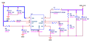
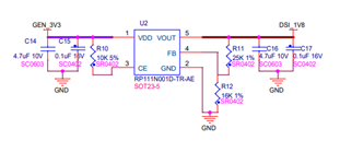
The bottom plate uses the DC 5.5 plug (P1) socket to insert the 5V power supply for power supply. After the C1 capacitor voltage stabilization filter, the self-recovery fuse (F1), (D2) 5.6V Zener diode and Q2 transistor control 5VDC-DC through the power input feedback detection ( Q1) The high and low level input of pin4 EN pin controls the power on and off to prevent the power input from overvoltage protection. The output 5VIN voltage of the latter stage is filtered by capacitors and magnetic beads and then stepped down by 3.3V and 1.8V in turn to supply power to some circuits of the control base plate.
Note:When designing the power supply part, please follow the minimum 3A current for copper cladding and power wiring, and for 1.8V, please follow the minimum 1.5A current for copper cladding and power wiring. Instantaneous overload leads to PCB burning, ensuring normal power supply.
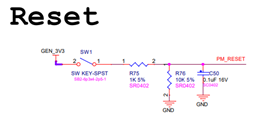
2. Reset circuit
Note:This development board reserves the hardware input reset, press the SW1 reset switch to pull up the 3.3V system reset.
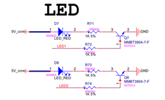
3. LED display circuit
There are 4 LED lights in this system.
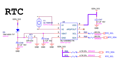
4. RTC real time clock circuit
The RTC chip used in this circuit has a built-in crystal oscillator matching capacitor. If you need to replace the solution, you need to pay attention to the crystal oscillator accuracy. You can connect the matching capacitor to the ground in parallel on the two crystal oscillator networks to meet the needs of adjustment accuracy. When the backplane is powered on, the 3.3V power supply of the backplane will supply power to the RTC chip and charge the battery BT1; when the backplane is powered off, the battery BT1 will discharge as the power supply for the RTC chip to work.
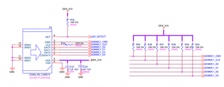
5. External TF card circuit
Note:The SDIO interface network on the right side of the figure is connected to the pull-up resistor. When designing the PCB, it is necessary to do equal-length processing and require 3W spacing and do overall package processing. When designing and developing, please connect pull-up resistors for all 7 SDCO signal lines。
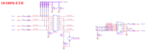
6. Ethernet circuit interface
Note:This module outputs a total of two Ethernet interfaces, of which the development board circuit ETH1 is the first group output of the module, and ETH2 is the second group output through the chip (IP101GR) to expand the network port output. Wiring requirements ETH TX/RX signal line PCB design needs to do equal-length processing and require 3W spacing and do overall wrapping processing. The differential pair and other networks must maintain a distance of more than 3 times the line width; the differential pair requires the equal-length error range within Within 5 mil, the equal-length error range between differential pairs is required to be within 25 mil, and the power supply part needs to thicken the filter capacitor as close to the terminal as possible. The copper-clad GND should avoid the bottom of the network transformer, and the U5/U12 ceramic gas discharge tube should be placed close to the RJ45 interface.
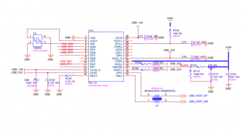
7. USB circuit
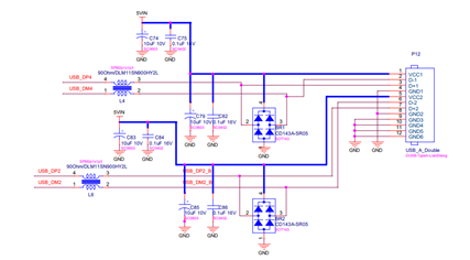
External 2-way USB input socket circuit
Note:The 5VIN power supply needs to strictly reserve at least 1.5A through the current design to be bold, and the DP/DM signal line needs to go through the differential signal line. BR1/2 are anti-static protection devices, L4/5/6 are common-mode filters, and need to be close to the USB interface when designing the PCB. P12 is a USB2.0 socket that can be connected to a USB flash drive or a mouse.
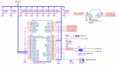
8. 4G module circuit
Note:The instantaneous working current of the 4G module can reach about 3A. When designing the circuit, the 3.3v power line should be designed strictly according to the current, and the filter capacitor should be placed as close as possible; D4 is the working status indicator of the module, and P27 is the SIM card holder. It is required to be placed close to the 4G module. , the module to the SIM card network requires grouped wiring to avoid the wiring being too far, the length error is too large, and it is far away from the strong signal interference source and the wiring needs to be arranged nearby. L12 is a common mode filter, and the USB cable requires differential routing.
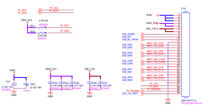
9. MIPI circuit
Note:The 5V/3.3V/1.8V power supply should be designed according to the current of more than 1A. Except for the power line, the other signal lines should be wired in strict accordance with the equidistant differential signal lines. Place close to the interface.
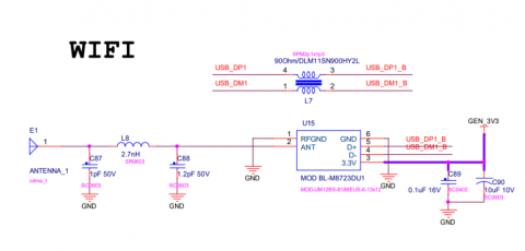
10. WIFI module circuit
Note: The 3.3V power supply needs to be designed according to the current above 1A, the USB signal line circuit needs to be routed strictly according to the same length, and the wiring should be routed as far as possible without punching holes. The output line from the ANT end of the module to the output signal end of the E1 antenna terminal should be widened as much as possible. The network where E1 is located requires the wiring to meet the 50Ω impedance design. Both ends of the antenna output should be covered with copper GND as much as possible.
11. SPI/I2C/AUD/GPIO/IRN circuit
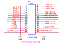
Pin header_AUD_GPIO_IRIN interface
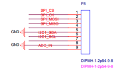
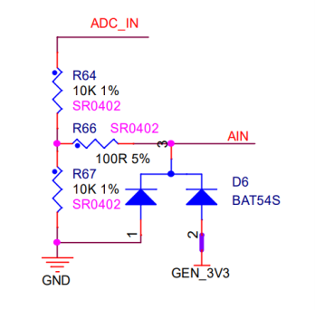
Pin header SPI, I2C, ADC interface
Note:Signal lines such as I2C and SPI should be routed strictly in accordance with differential lines and should be as short as possible and wrapped around the lines to avoid interference such as signal lines.
12. RS232/485 circuit
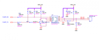
Note:The 3.3V power supply needs to be designed according to the current above 1A, and the TX/RX signal line circuit needs to be wired strictly according to the equidistant differential signal line. P5 is the internal debugging port. For the convenience of later debugging, please lead out this debugging serial port when designing the backplane by yourself. The 485 signal terminal matching resistor R58 is increased by 120 ohms depending on the number of loads and the transmission length. When the device is laid out, the U6 and U7 chips are placed close to the P6 and P7 interfaces.
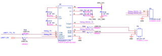
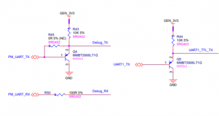
13. Debug serial port and programming interface
Note:When designing the PCB, the two signal lines of each TX/RX should be routed in groups to avoid too much error in the length of the two network lines in the group when the lines are too far away.
PCB Design Requirements:
1、When the overall layout is made, the power supply and functional modules should be laid out separately. The module should be used as a unit. The unshielded modules should be as close as possible, and the signal traces should be as short as possible.
2、If there is a shielding requirement, the module needs to be shielded, and the surrounding is wrapped with GND, and the GND should be as large as possible to make more holes.
3、The wiring of the power supply part should be thickened as much as possible, and the forks and holes should be made as small as possible. Capacitors and inductors should be placed as close to the power supply and IC as possible.
