MYZR-LS1012A-MB200 hardware introduction
目录
- 1 Interface Overview
- 2 Interface functions
- 2.1 Two-digit DIP switch
- 2.2 Reset switch
- 2.3 Debug serial port
- 2.4 232 serial port & 485 serial port
- 2.5 DI extension
- 2.6 DO extension
- 2.7 GPIO&PMU control
- 2.8 4G mini-PCIE & SIM Deck
- 2.9 K20-JTAG
- 2.10 SD Deck
- 2.11 USB Extension
- 2.12 Main power input & switch
- 2.13 Ethernet
- 2.14 LORA Module
- 2.15 WIFI/BT Module
- 2.16 ZIGBEEModule
Interface Overview
Front view

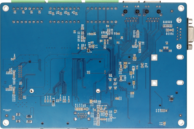
Rear view(MB200)

Dimensions(MB200)

Interface functions
Two-digit DIP switch
silk screen:SW1
The pins and signals are defined as follows:

| Mode control | 1 bit | 2 bit |
| Flash mode | x | 0 |
| Startup mode | x | 1 |
Reset switch
Silkscreen: SW2
Function: press reset
Debug serial port
Silk screen: P1
Interface attributes: UART0, RS-232 level
The pins and signals are defined as follows:

232 serial port & 485 serial port
Silk screen:J1
| Name | Quantity | Interface Properties |
| RS-232 | 3 | USB extended serial port with data rate up to 235Kbps |
| RS-485 | 3 | USB extended serial port with data rate up to 12Mbps |
The pins and signals are defined as follows:

DI extension
Silk screen: J2
Interface attributes: extended DI, optocoupler isolation
The pins and signals are defined as follows:

DO extension
Silkscreen: J3
Interface attributes: extended DO, optocoupler isolation
The pins and signals are defined as follows:

GPIO&PMU control
Silkscreen: J4
Interface attributes: spare pins, some can be used as GPIO
The pins and signals are defined as follows:

| Pin | Signal | Description | Pin | Signal | Description |
| J4-1 | INT_PMU | Core board PMU interrupt request output | J4-2 | DUT_SAI2_RX_SYNC | Core board leads, can be used as GPIO |
| J4-3 | HRESET_PMU | Pull out of core board, can be used as GPIO | J4-4 | DUT_SAI2_RX_BCLK | Core board leads, can be used as GPIO |
| J4-5 | PMU_GPIO1 | Pull out of core board, can be used as GPIO | J4-6 | GND | DGND |
| J4-7 | PMU_GPIO0 | Pull out of core board, can be used as GPIO | J4-8 | GND | DGND |
| J4-9 | PMU_GPIO2 | Pull out of core board, can be used as GPIO | J4-10 | GND | DGND |
| J4-11 | PMU_SLEEP | Core board PMU standby mode control signal input | J4-12 | GND | DGND |
4G mini-PCIE & SIM Deck
| Name | Screen Printing | Interface Properties |
| 4G mini-PCIE | J5 | miniPCIE standard interface, PCIe 2.0 standard |
| SIM card holder | P2 | Connect 4G SIM Card |
The pins and signals are defined as follows:


K20-JTAG
Silkscreen: J8
Interface attributes: K20-JTAG programming module interface
The pins and signals are defined as follows:

| Pin | Signal | Description | Pin | Signal | Description |
| J8-1 | DUT_UART_SOUT | Debug serial output | J8-2 | PROC_TMS | Test Mode Selection |
| J8-3 | DUT_UART_SIN | Debug serial input | J8-4 | PROC_TCK | Test Clock Output |
| J8-5 | LSJTAG_TRST_B | LS1012A reset signal | J8-6 | PROC_TDO | Test data output |
| J8-7 | VCC_1V8 | 1.8V output | J8-8 | PROC_TDI | Test Data Entry |
| J8-9 | GND | Digitally | J8-10 | SDA_RST_TGTMCU | K20 reset signal |
| J8-11 | GND | Digitally | J8-12 | GND_DETECT | Ground Detection |
SD Deck
Silkscreen: J9
Interface attributes: standard SD card socket, support SD3.01, speed is UHS-1 standard
The pins and signals are defined as follows:

USB Extension
Silkscreen: J10
Interface attributes: USB1 expansion USB3.0 + USB2.0, USB TYPE-A interface
The pins and signals are defined as follows:

Main power input & switch
| Name | Screen Printing | Interface Properties |
| Main Power Input | J11 | Internal positive external negative jack, 5V voltage |
| Main Power Switch | J12 | Power Switch |
The pins and signals are defined as follows:

Ethernet
| Name | Screen Printing | Interface Properties |
| Ethernet Port 1 | U1 | ETH1, SGMII, support 10/100 / 1000M |
| Ethernet port 0 | U2 | ETH0, SGMII, support 10/100 / 1000M |
The pins and signals are defined as follows:


LORA Module
Silkscreen: U23
Interface attributes: LORA module, serial communication
The pins and signals are defined as follows:

| Pin | Signal | Attribute |
| U23-1、2、3、4、11、13、19、20、22 | GND | DGND |
| U23-12、14、15、16、17、18、21 | NC | Dangling |
| U23-10 | 5VIN | Module 5V input |
| U23-9 | LoRa_AUX | Module working status indication |
| U23-8 | LoRa_RX | Module TTL serial input |
| U23-7 | LoRa_TX | Module TTL serial output |
| U23-6 | LoRa_M1 | Module Working Mode Control |
| U23-5 | LoRa_M0 | Module Working Mode Control |
WIFI/BT Module
Silkscreen: U24
Interface attributes: WIFI / BT module, USB communication
The pins and signals are defined as follows:

| Pin | Signal | Attribute |
| U24-1 | GND | DGND |
| U24-2 | ANT | Antenna interface |
| U24-3 | VCC_3.3V | Module 3.3V Input |
| U24-4 | WIFI_USBDM | USB data positive |
| U24-5 | WIFI_USBDP | USB data negative |
| U24-6 | GND | DGND |
ZIGBEEModule
Silkscreen: U26
Interface attributes: ZIGBEE module, serial communication
The pins and signals are defined as follows:

| Pin | Signal | Attribute | Pin | Signal | Attribute |
| U26-1 | GND | DGND | U26-11 | ZigBee_TX | Module TTL serial input |
| U26-2 | VCC_3.3V | Module 3.3V Input | U26-12 | RUN_LED | Indicate module normal operating status |
| U26-6 | ZigBee_Baud_RST | Restore the serial baud rate of 115200 | U26-13 | NWK_LED | Indicate module network access status |
| U26-7 | ZigBee_AT_HEX | Switch instruction mode | U26-24 | ZigBee_nRST | Module Reset |
| U26-10 | ZigBee_RX | Module TTL serial output |