MY-IMX6 Hardware Development Guide
This document is for users to have a quick design of base board,with guidance for how to solve the questions clients may meet commonly,in order for clients to design a product which can be used in all kinds of environments.
目录
Power supply
Schematic
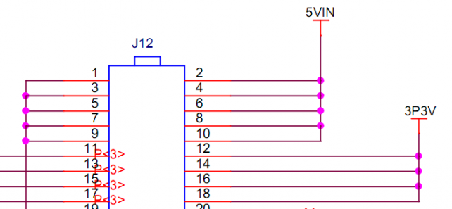
- MY-I.MX6 series of core board only needs 5V power source(constant current is not small than 2A,peak value 2.5A-3A)as an input。details as below.
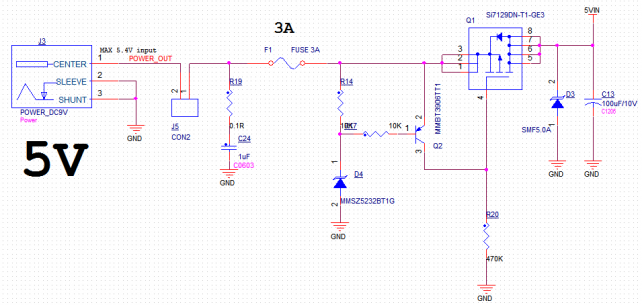
- If it is a direct 5V input,5V power source need a over voltage protection,the protection circuit can be designed with following reference.
- If it is high voltage input to be converted to 5V through DCDC principle,the core board will output 3P3V power source with a maximum current 500mA of which can be used as power supply for base board if current with 3.3V on the base board is too small,in this case,please put in serial a fuse for this 3P3V power source .
- Since current with 3.3V on the base board is usually over 500mA,normally users will generate a another 3.3V through DCDC or LDO.
Note:enable control must be done for 3.3V on base board by 3P3V on core board instead of being conducted by other power sources on the base board.if there are other power sources on base board,their enable controls must be conducted by 3P3V as well,this is up to the nature of I.MX6 chip.
Reference circuit as below:
642px
PCB
- Capacitor with big capacity should be placed near 5V input on core board, to ensure contituous power supply even when sudden extra load is added for CPU。if there is via hole,need to make sure via hole can go through 3A peak current,more via holes can be built to increase current.
Serial port design
Principle
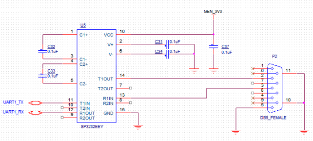
- For serial port design,common questions arising are inversion between RXD and TXD。network standard in the schematic as below.
- TXD——CPU output
- RXD——CPU input
- TXD——CPU output
PCB
Note:we can provide schematic and PCB diagram for design of base board,our serial port is female head as connector.please assure your design to be consistent with our offer,if change serial port to be male head connector,then RS232 siganl connector head need to be changed accordingly.For the details of male and female head connector,please get on internet for consuls.
SD card design
Principle
- For users'design of SD card,please follow strictly schematic to arrange IO dropdown,excessive dropdown will enable SD card not to work normally。reference diagram as below.
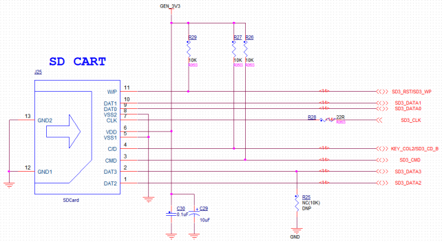
Note:If users don't need SD card,but need TF card,since TF card doesn't have function of write-protect.Write-protect signal(SD3_RST/SD3_WP)need to pull down,which can't be hanged direclty in the air.If TF card booth is designed with hot swap,must make clear which pin of TF card is for dectetion。normally when insert the card,detection pin will be grounded,the inserted detection pin KEY_COL/SD3_CD_B)need to pull up.If TF card booth is designed with flip type,write-protect need to pull up,at the same time the inserted detection signal need to be grounded(just as a card is kept in the booth).
- If need additional ESD protect,please ensure a small capacity value on SD_CLK signal.
- If need additional ESD protect,please ensure a small capacity value on SD_CLK signal.
PCB
SD0,SD1,SD2,SD3,CMD,CLK signal need an equal treatment。ESD originals need to be very close to SD card booth.
SATA design
Principle
- SATA principle is simple by contrast, only need to ensure a correct direction. since current on SATA is normally a little big, 5V current inputed is better not to be as low as 3A.
PCB
- The four capacitors which are serialed to SATA signal should be close to SATA booth.
- 100 ohm difference resistance matching up.
- Length tolerance for each group of differences pairs is controlled within ±5mil.
- Require a full reference to ground level.
HDMI
Principle
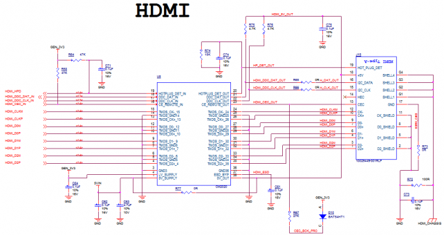
HDMI stand can't be linked with wrong definition.
PCB
- 100 ohm difference resistance matching up.
- Length tolerance for each group of differences pairs is controlled within±5mil.
- Require a full reference to ground level.
- Protect component CM2020 can't be ignored.
LVDS
Principle
- If the LVDS signal is transmitted at a relatively long distance, the connected screen is relatively large, and the LVDS signal can be coupled in series to ensure better quality of transmission.
PCB
- 100 ohm difference resistance matching up.
- Length tolerance for each group of differences pairs is controlled within±5mil.
- If two way LVDS singla is used for 1080p displa,。LVDS0 and LVDS1 signal need an equal treatment.
- Require a full reference to ground level.
RGB port LCD
Principle
- LCD as RGB port need to be matched up with interface model with 24bit,18bit.
| CPU signal(note1) | 24bit(note2) | 18bit(note3) | 18bit(note4) |
| D0 | B0 | B0 | |
| D1 | B1 | B1 | |
| D2 | B2 | B0 | B2 |
| D3 | B3 | B1 | B3 |
| D4 | B4 | B2 | B4 |
| D5 | B5 | B3 | B5 |
| D6 | B6 | B4 | G0 |
| D7 | B7 | B5 | G1 |
| D8 | G0 | G2 | |
| D9 | G1 | G3 | |
| D10 | G2 | G0 | G4 |
| D11 | G3 | G1 | G5 |
| D12 | G4 | G2 | R0 |
| D13 | G5 | G3 | R1 |
| D14 | G6 | G4 | R2 |
| D15 | G7 | G5 | R3 |
| D16 | R0 | R4 | |
| D17 | R1 | R5 | |
| D18 | R2 | R0 | |
| D19 | R3 | R1 | |
| D20 | R4 | R2 | |
| D21 | R5 | R3 | |
| D22 | R6 | R4 | |
| D23 | R7 | R5 |
- Note1.
- D0 indicate a minimal level for CPU liquid crystal port
- D23 indicate a maximal level for CPU liquid crystal port
- Note2.
- B0-24 bit blue bit of liquid crystal at minimal level,
- B7-24 bit blue bit of liquid crystal at maximal level,
- G0-24 bit green bit of liquid crystal at minimal level,
- G7-24 bit green bit of liquid crystal at maximal level,
- R0-24 bit red bit of liquid crystal at minimal level,
- R7-24 bit red bit of liquid crystal at maximal level
- Note3..
- In use of this kind of link,LCD software still choose 24bit model,
- B0-18 bit blue bit of liquid crystal at minimal level,
- B5-18 bit blue bit of liquid crystal at maximal level,
- G0-18 bit green bit of liquid crystal at minimal level,
- G5-18 bit green bit of liquid crystal at maximal level,
- R0-18 bit red bit of liquid crystal at minimal level,
- R5-18 bit red bit of liquid crystal at maximal level,
- Note 4.
- If in use of this link method,LCD software need to choose 18bit model,
- B0-18 bit blue bit of liquid crystal at minimal level,
- B5-18 bit blue bit of liquid crystal at maximal level,
- G0-18 bit green bit of liquid crystal at minimal level,
- G5-18 bit green bit of liquid crystal at maximal level,
- R0-18 bit red bit of liquid crystal at minimal level,
- R5-18 bit red bit of liquid crystal at maximal level,
- If there is a strict request with static,need ESD protect for LCD signal.
PCB
- For all data lines,need an equal treatment for CLK signal.
- Request a full reference to ground level.
CMOS
Principle
PCB
- Since frequency of MCLK and PIXCLK signal is very high,need isolation treatment when Layout,
- Data,need an equal treatment for clk signal,
- Request a full reference to ground level,
USB
Principle
- USBHOST expanded with 4 and USBHOST via LAN9514,and expanded with one way 10M/100M ethernet interface.
- A coupling inductance is put in serial on USB line.
- The USB _ H1_VBUS signal of the core plate is connected to the 5V power supply through the magnetic bead.
- If power supply Host out of the board,please include over-current protect component for USD.

So far only device port can be done in layout of hardware for MINIUSB port,if need function of HOST,please refer to OTG layout from FSL official.
PCB
- 90 ohm difference resistance matching up
- Request a full reference to ground level
- Current to supply outside need to be big enough.
CAN
Principle
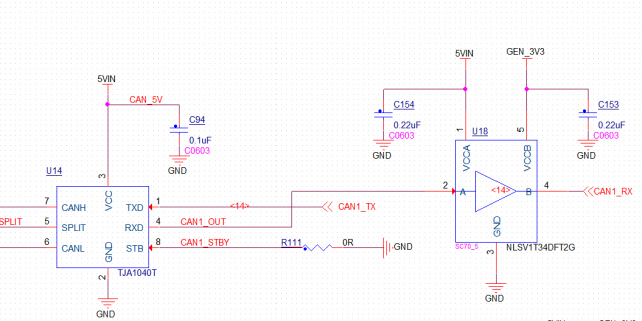
Since CAN的TX,RX signal is 3.3V electrical level,attention to conversion of electrical level.
PCB
CANH,CANL check signal.
PCIE
Principle
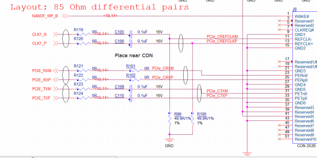
- TX,RX signal need to connect in serial with 0.1uF capacitor(if an external module is already with a capacitor in serial,then no need to connect a capacitor again)
- CLK signal connect in serial with 0.1uF capacitor,at the same time put a 49.8 resistor to ground in parallel with another end of the capacitor .
PCB
- 85 ohm difference resistance matching up
- Request a full reference to ground level
