MYZR-I.MX8Mmini hardware introduction
目录
- 1 ==Interface overview==
- 2 Front view
- 3 Back view
- 3.1 Dimensional drawing
- 3.2 =Interface function=
- 3.3 WIFI/BT antenna
- 3.4 TF card
- 3.5 Debug serial port
- 3.6 MIPI_DSI interface
- 3.7 MIPI_CSI interface
- 3.8 MINI_PCIe/4G&SIM card
- 3.9 Audio interface
- 3.10 BOOT MODE switch
- 3.11 Reset switch
- 3.12 Extended IO interface
- 3.13 Main power switch
- 3.14 Bootloader interface
- 3.15 USB extended serial port RS-485&RS-232
- 3.16 USB extension USB HOST
- 3.17 Ethernet interface
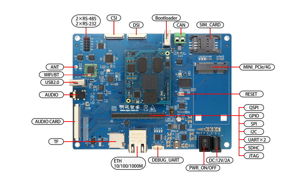
==Interface overview==
Front view
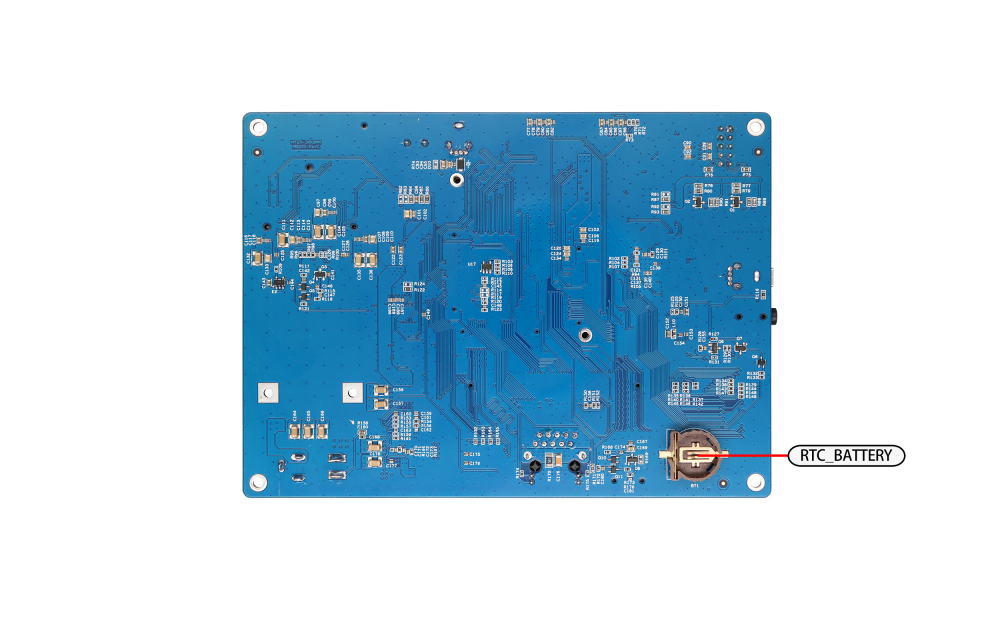
Back view
Dimensional drawing
=Interface function=
WIFI/BT antenna
Silkscreen: ANT
Pins and signals are defined as follows:

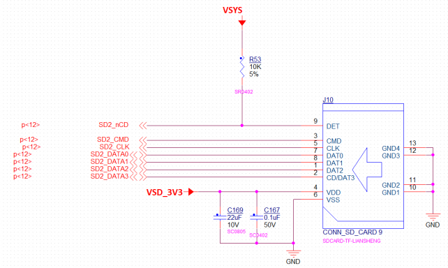
TF card
Silkscreen: J10 Pins and signals are defined as follows:
Debug serial port
Silkscreen: J12
Pins and signals are defined as follows:
| Pin used | Function |
|---|---|
| UART4_TXD | MCU debug serial port data output |
| UART2_TXD | CPU debug serial port data output |
| UART4_RXD | MCU debug serial port data reception |
| UART2_RXD | CPU debug serial port data reception |
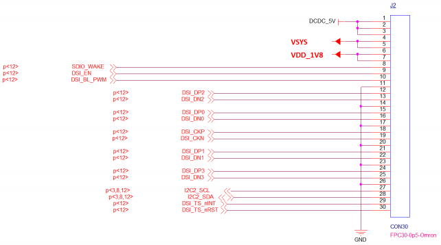
MIPI_DSI interface
Silkscreen: J2
The pins and signals are defined as follows:
| Pin | signal | description | pin | signal | description |
|---|---|---|---|---|---|
| J2-1 | DCDC_5V | 5V output | J2-16 | DSI_DN0 | DSI differential data 0 |
| J2-2 | J2-17 | GND | Digital Ground | ||
| J2-3 | J2-18 | DSI_CKP | DSI differential clock | ||
| J2-4 | VDD_3V3 | 3.3V output | J2-19 | DSI_CKN | DSI differential clock |
| J2-5 | J2-20 | GND | Digital ground | ||
| J2-6 | VDD_1V8 | 1.8V output | J2-21 | DSI_DP1 | DSI differential data 1 |
| J2-7 | J2-22 | DSI_DN1 | DSI differential data 1 | ||
| J2-8 | SDIO_WAKE | GPIO control | J2-23 | GND | Digital ground |
| J2-9 | DSI_EN | GPIO control | J2-24 | DSI_DP3 | DSI differential data 3 |
| J2-10 | DSI_BL_PWM | GPIO control | J2-25 | DSI_DN3 | DSI differential data 3 |
| J2-11 | GND | Digital Ground | J2-26 | GND | Digital Ground |
| J2-12 | DSI_DP2 | DSI differential data 2 | J2-27 | I2C3_SCL | Touch I2C signal |
| J2-13 | DSI_DN2 | DSI differential data 2 | J2-28 | I2C3_SDA | Touch I2C signal |
| J2-14 | GND | Digital ground | J2-29 | DSI_TS_nINT | GPIO control |
| J2-15 | DSI_DP0 | DSI differential data 0 | J2-30 | DSI_TS_nRST | GPIO control |
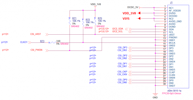
MIPI_CSI interface
Silkscreen: J1
Pins and signals are defined as follows:

| Pin | Signal | Description | Pin | Signal | Description |
|---|---|---|---|---|---|
| J3-1 | DCDC_5V | 5V input | J3-16 | CSI_P1_DP3 | CSI differential data 3 |
| J3-2 | --- | --- | J3-17 | CSI_P1_DN3 | CSI differential data 3 |
| J3-3 | VDD_1V8 | 1.8V input | J3-18 | GND | Digital ground |
| J3-4 | --- | --- | J3-19 | CSI_P1_DP2 | CSI differential data 2 |
| J3-5 | VDD_3V3 | 3.3V input | J3-20 | CSI_P1_DN2 | CSI differential data 2 |
| J3-6 | --- | --- | J3-21 | GND | Digital Ground |
| J3-7 | GND | Digital ground | J3-22 | CSI_P1_DP1 | CSI differential data 1 |
| J3-8 | GND | Digital ground | J3-23 | CSI_P1_DN1 | CSI differential data 1 |
| J3-9 | I2C1_SDA_1V8 | I2C signal, 1.8V | J3-24 | GND | Digital ground |
| J3-10 | I2C1_SCL_1V8 | I2C signal, 1.8V | J3-25 | CSI_P1_CKP | CSI differential clock |
| J3-11 | CSI_nRST | GPIO control | J3-26 | CSI_P1_CKN | CSI differential clock |
| J3-12 | CSI_P1_PWDN | GPIO control | J3-27 | GND | Digital ground |
| J3-13 | GND | Digital ground | J3-28 | CSI_P1_DP0 | CSI differential data 0 |
| J3-14 | CSI1_CLK | CSI clock | J3-29 | CSI_P1_DN0 | CSI differential data 0 |
| J3-15 | GND | Digital Ground | J3-30 | GND | Digital Ground |
Pins and signals are defined as follows:
MINI_PCIe/4G&SIM card
| Name | Silkscreen | Interface attributes |
|---|---|---|
| mini-PCIE/4G | J6 | miniPCIE standard interface, PCIe 2.0 standard, support 4G module |
| SIM card holder | CON1 | 4G SIM card holder |
Pins and signals are defined as follows:
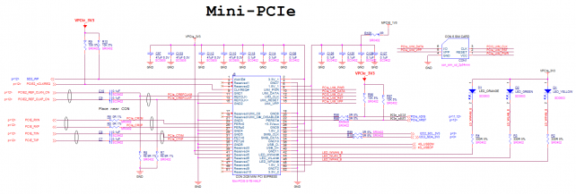
| Pin | signal | description | pin | signal | description |
|---|---|---|---|---|---|
| J6-1 | SD2_WP | GPIO control | J6-2 | 3.3V_1 | 3.3V power supply |
| J6-3 | NC | --- | J6-4 | GND7 | GND |
| J6-5 | NC | --- | J6-6 | 1.5V_1 | 1.5V power supply |
| J6-7 | PCIE2_nCLKREQ | PCIE clock request | J6-8 | PCIe_UIM_PWR | PCIe_UIM_PWR |
| J6-9 | GND1 | GND | J6-10 | PCIe_UIM_DATA | PCIe_UIM_DATA |
| J6-11 | PCIE2_REF_CLKN_CN | PCIE reference clock | J6-12 | PCI3_UIM_CLK | PCI3_UIM_CLK |
| J6-13 | PCIE2_REF_CLKP_CN | PCIE reference clock | J6-14 | PCIe_UIM_RST | PCIe_UIM_RST |
| J6-15 | GND2 | GND | J6-16 | PCIe_UIM_VPP | PCIe_UIM_VPP |
| J6-17 | NC | --- | J6-18 | GND8 | GND |
| J6-19 | NC | --- | J6-20 | PCIe_nDIS | PCIE prohibition control |
| J6-21 | GND3 | GND | J6-22 | PCIe_nRST | PCIE total |
| J6-23 | PCIE_RXN | PCIE data receiving | J6-24 | +3.3Vaux | 3.3V power supply |
| J6-25 | PCIE_RXP | PCIE data receiving | J6-26 | GND9 | GND |
| J6-27 | GND4 | GND | J6-28 | 1.5V_2 | 1.5V power supply |
| J6-29 | GND5 | GND | J6-30 | I2C2_SCL_3V3 | I2C signal |
| J6-31 | PCIE_TXN | PCIE data output | J6-32 | I2C2_SDA_3V3 | I2C signal |
| J6-33 | PCIE_TXP | PCIE data output | J6-34 | GND10 | GND |
| J6-35 | GND6 | GND | J6-36 | 4G_USBDM | USB differential signal |
| J6-37 | Reserved3 | connect to GND | J6-38 | 4G_USBDP | USB differential signal |
| J6-39 | Reserved4 | connect to 3.3V | J6-40 | GND11 | GND |
| J6-41 | Reserved5 | connect to 3.3V | J6-42 | LED_WWAN_B | LED indicator |
| J6-43 | Reserved6 | connect to GND | J6-44 | LED_WLAN_B | LED indicator |
| J6-45 | Reserved7 | NC | J6-46 | LED_WPAN_B | LED indicator |
| J6-47 | Reserved8 | NC | J6-48 | 1.5V_3 | 1.5V power supply |
| J6-49 | Reserved9 | NC | J6-50 | GND12 | GND |
| J6-51 | Reserved10 | NC | J6-52 | 3.3V_2 | 3.3V power supply |
Audio interface
Silkscreen: P4
Pins and signals are defined as follows:
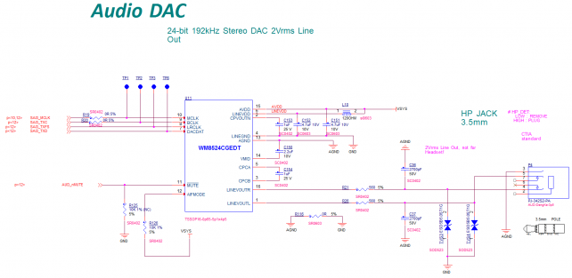
| Pin used | Function |
|---|---|
| SAI3_MCLK | Master clock |
| SAI3_TXC | Digital Audio Bit Clock |
| SAI3_TXFS | Digital audio left/right clock |
| SAI3_TXD | Digital audio data output |
| AUD_nMUTE | Mute enable |
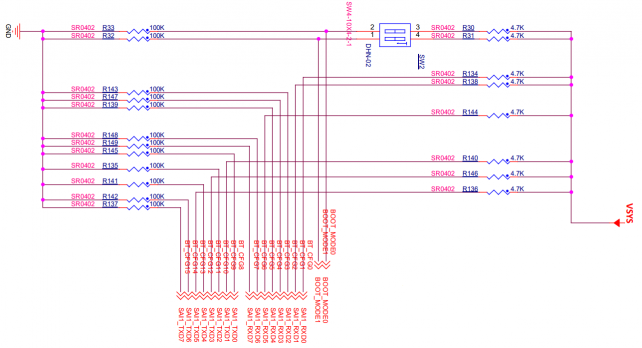
BOOT MODE switch
Silkscreen: SW2 Pins and signals are defined as follows:
| Mode control | 1 bit | 2 bit |
|---|---|---|
| Programming mode | 0 | 1 |
| Start mode | 1 | 0 |
Reset switch
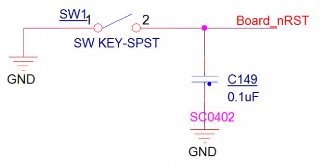
Silkscreen: SW1
Function: Press to reset
Pins and signals are defined as follows:
Extended IO interface
Silkscreen: J7
Pins and signals are defined as follows:
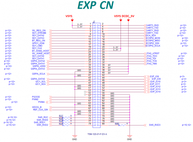
| Pin | Signal | Pin | Signal |
|---|---|---|---|
| J7-1 | VSYS | J7-2 | UART3_RXD |
| J7-3 | J7-4 | UART3_TXD | |
| J7-5 | WL_REG_ON | J7-6 | UART1_RXD |
| J7-7 | SD1_STROBE | J7-8 | UART1_TXD |
| J7-9 | SD1_DATA2 | J7-10 | I2C4_SDA |
| J7-11 | SD1_DATA3 | J7-12 | ECSPI2_MOSI |
| J7-13 | BT_REG_ON | J7-14 | ECSPI2_MISO |
| J7-15 | GPIO1_IO08 | J7-16 | ECSPI2_SS0 |
| J7-17 | SD1_CMD | J7-18 | ECSPI2_SCLK |
| J7-19 | SD1_CLK | J7-20 | 3.3V |
| J7-21 | BT_WAKE_HOST | J7-22 | |
| J7-23 | WL_WAKE_HOST | J7-24 | JTAG_nTRST |
| J7-25 | SD1_DATA0 | J7-26 | JTAG_TDO |
| J7-27 | SD1_DATA1 | J7-28 | JTAG_TDI |
| J7-29 | QSPIA_DATA2 | J7-30 | JTAG_TCK |
| J7-31 | QSPIA_DATA1 | J7-32 | JTAG_TMS |
| J7-33 | QSPIA_nSS0 | J7-34 | 5V |
| J7-35 | QSPIA_DATA3 | J7-36 | |
| J7-37 | GND | J7-38 | |
| J7-39 | QSPIA_SCLK | J7-40 | |
| J7-41 | GND | J7-42 | EXP_IO8 |
| J7-43 | QSPIA_DATA0 | J7-44 | EXP_IO9 |
| J7-45 | I2C1_SCL | J7-46 | EXP_IO10 |
| J7-47 | I2C1_SDA | J7-48 | EXP_IO11 |
| J7-49 | GND | J7-50 | EXP_IO12 |
| J7-51 | GND | J7-52 | EXP_IO13 |
| J7-53 | NC | J7-54 | EXP_IO14 |
| J7-55 | NC | J12-56 | GND |
| J7-57 | PGOOD | J12-58 | |
| J7-59 | PWM2 | J12-60 | |
| J7-61 | PWM4 | J12-62 | |
| J7-63 | GND | J12-64 | |
| J7-65 | WDOG_B | J12-66 | |
| J7-67 | REF_CLK_32K | J12-68 | |
| J7-69 | GND | J12-70 | |
| J7-71 | GND | J12-72 | |
| J7-73 | SAI5_RXC | J12-74 | |
| J7-75 | SAI5_RXD0 | J12-76 | |
| J7-77 | SAI5_RXD1 | J12-78 | |
| J7-79 | SAI5_RXD2 | J12-80 | SAI5_RXD3 |
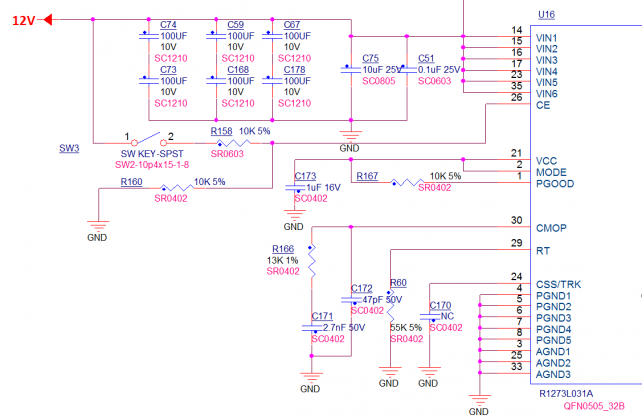
Main power switch
Silkscreen: SW3 Pins and signals are defined as follows:
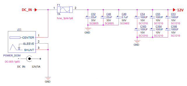
Main power input
Silkscreen: J11
Interface attributes: internal positive and external negative jacks, 12V voltage
Pins and signals are defined as follows:
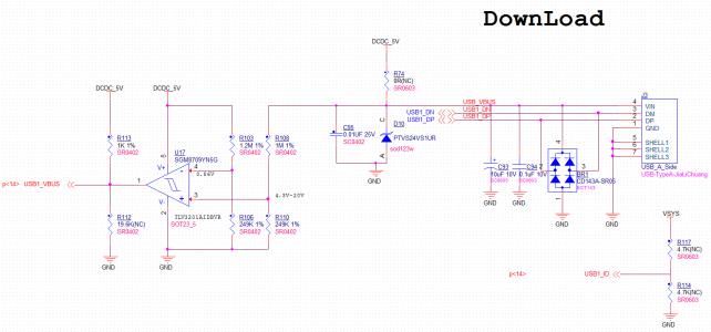
Bootloader interface
Silkscreen: J3
Pins and signals are defined as follows:
| Pin used | Function |
|---|---|
| USB1_VBUS | VBUS detection |
| USB1_DN | USB differential data |
| USB1_DP | USB differential data |
| USB1_ID | NC |
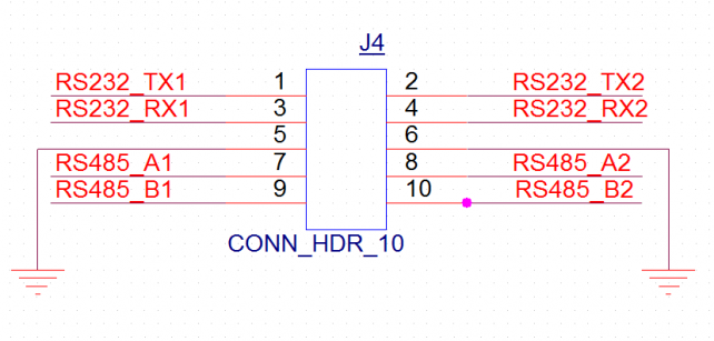
USB extended serial port RS-485&RS-232
Silkscreen: J4
Pins and signals are defined as follows:
| Pin | Signal | Pin | Signal |
|---|---|---|---|
| RS232_TX1 | RS-232 signal output | RS232_RX1 | RS-232 signal receiving |
| RS232_TX2 | RS-232 signal output | RS232_RX2 | RS-233 signal receiving |
| RS482_A1 | RS-485 differential signal + | RS482_B1 | RS-485 differential signal- |
| RS482_A2 | RS-485 differential signal + | RS482_B2 | RS-485 differential signal- |
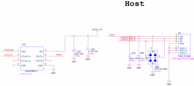
USB extension USB HOST
Silkscreen: J5
Interface attributes: USB2 extended USB2.0
Pins and signals are defined as follows:
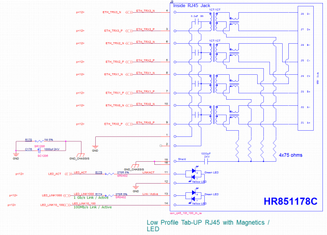
Ethernet interface
Silkscreen: J9
Interface attributes: RGMII, support 10/100/1000M
引脚及信号定义如下:
